
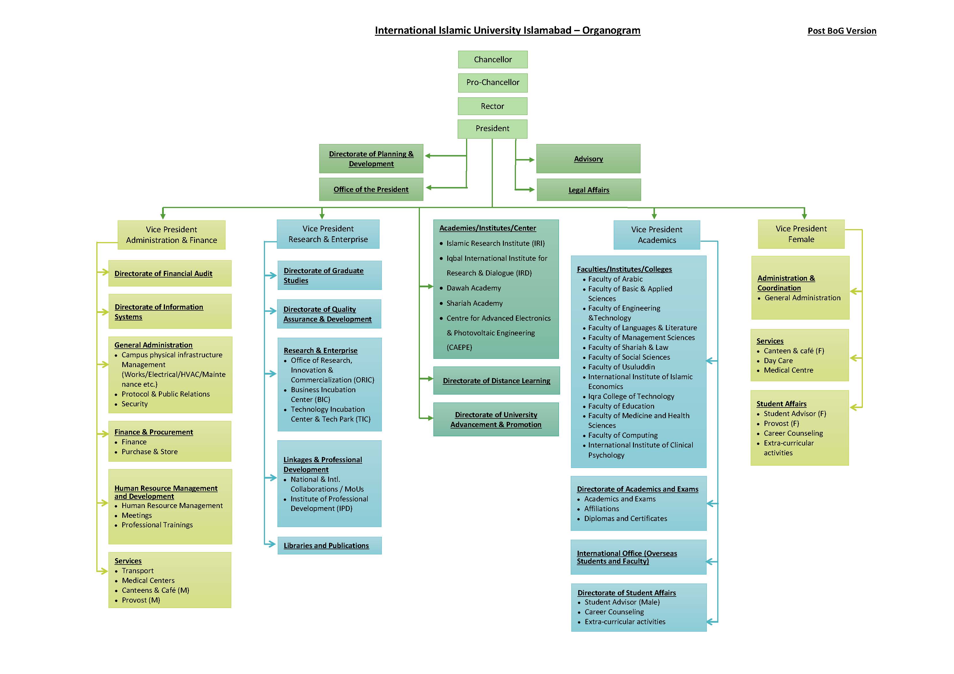
The IDB-IIU Advanced Electronics Laboratories International Islamic University Islamabad under the umbrella of Center of Advanced Electronics & Potovoltaic Engineering (CAEPE) conducted its 4th 6-days workshop on “CHIP PROCESS DESIGN AND ANALYTICAL TESTING” for faculty members and graduate students who entered into research phase.
T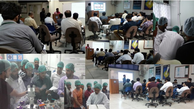 he workshop took place in both the research laboratories namely Device Design Suite and Process Characterization Suite. The training was conducted on internationally licensed softwares and R&D grade sophisticated machines in the laboratories. The workshop was over six hands-on teaching and training sessions including Chip Design’s Physical Processes, Electrical Characterization, Advanced Electrical Characterization, Electro-optical Assessment & Rapid Thermal Processing, and Back End Processes.
The team of trainers led by Prof. Dr. Ahmed Shuja Syed (Executive Director CAEPE), Engr. Faraz Qayyum, Engr. Shoaib Alam and Engr. Muhammad Ali provided the participants with the knowledge and tools of physical processes of IC design as well as post-process reliability, efficiency and failure analysis of devices and micro-systems for diverse applications.
The workshop was designed in such a way, that the attendees got the maximum interaction with the available techniques in the lab. First two days were focused on the industry driven licensed softwares for both the physical and the circuit level designing and integration of the Micro Systems. 3rd and the 4th days were planned on the extremely sophisticated electrical and electro-optical characterization machines to seek the electrical behavioral parameters for the reliability assessment of the devices. The 5th day was comprised of the fab driven optical quantification and the annealing processes to map the fabricated devices optical parameters and also to see the impact of calculated heat flux on to the device activation and inner dynamics. The last day introduced the attendees with the novel contact metallization technique of Atomistic Layer physical Vapor Deposition system. The audience was also given the hands-on exercises of etching, cleaning, dicing and slicing of the wafers.